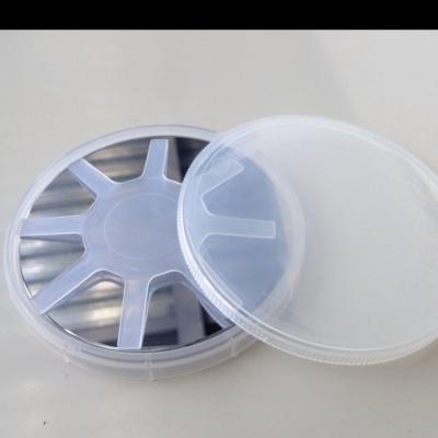
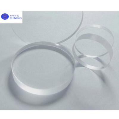
Gaufrette de phosphure d'indium
(33)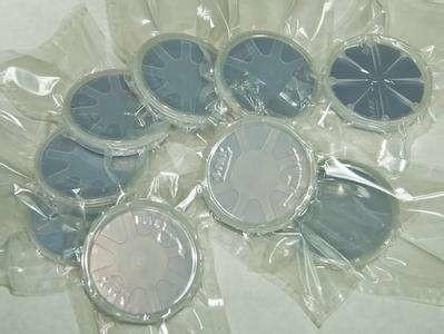
Gaufrette noire de phosphure d'indium, gaufrette de semi-conducteur pour l'application de LD
Prix: by case
MOQ: 5pcs
Heure de livraison: 1-4weeks
Marque: zmkj
Souligner:substrat de MgO, Gaufrette de Gap
substrats d'INP de 2inch 3inch 4inch pour l'application de LD, gaufrette de semi-conducteur, gaufrette d'INP, gaufrette de monocristal
L'INP présentent
Monocristal d'INP
La croissance de tCZ (méthode modifiée de Czochralski) est employée pour tirer un monocristal pa... Voir plus
➤ Visiter Site Internet
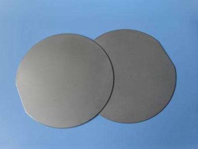
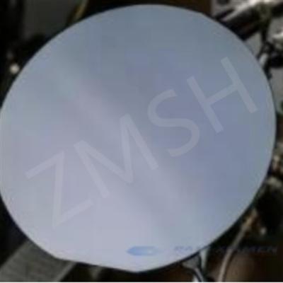
Matériel de semi-conducteur de plats de GE excellent d'indium de gaufrette optique de phosphure
Prix: by case
MOQ: 3pcs
Heure de livraison: 1-4weeks
Marque: zmkj
Souligner:substrat de MgO, Gaufrette de Gap
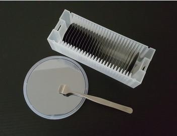
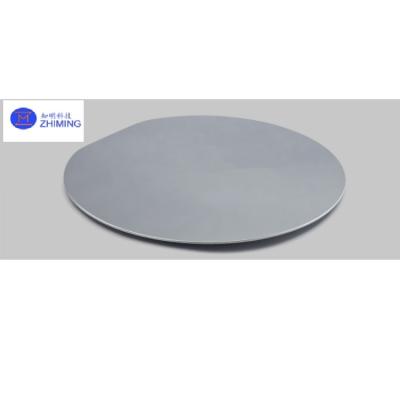
Gaufrettes de monocristaux de germanium, plats optiques de GE
Substrats de germanium
Application : gaufrette de germanium utilisée dans la production du dispositif de semi-conducteur, circuit optique de rayon infrarouge, matériel de descente de pile solaire.
Termes principaux de propr... Voir plus
➤ Visiter Site Internet
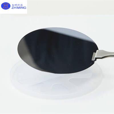
Gaufrette de phosphure de gallium d'indium d'INP de substrats de semi-conducteur de lentille de GE
Prix: by case
MOQ: 3pcs
Heure de livraison: 1-4weeks
Marque: zmkj
Souligner:Gaufrette de phosphure d'indium de lentille de GE, gaufrette de phosphure d'indium de substrats de semi-conducteur, monocristal de GE d'INP
gaufrettes de substrats de GE de monocristaux de germanium de 4inch 6inch, lentille optique adaptée aux besoins du client de GE
Substrats de germanium
Application : gaufrette de germanium utilisée dans la production du dispositif de semi-conducteur, circuit optique de rayon infrarouge, matéri... Voir plus
➤ Visiter Site Internet
Gaufrette semi-isolante d'INP de phosphure d'indium de 4 pouces pour la diode laser de LD
Prix: by case
MOQ: 10pcs
Heure de livraison: 3-4weeks
Marque: zmkj
Souligner:gaufrette d'INP, substrat de MgO
gaufrette semi-isolante d'INP de phosphure d'indium 4inch pour la diode laser de LD, gaufrette de semi-conducteur, gaufrette d'INP 3inch, substrats d'INP du monocristal wafer2inch 3inch 4inch pour l'application de LD, gaufrette de semi-conducteur, gaufrette d'INP, gaufrette de monocristal
L'INP... Voir plus
➤ Visiter Site Internet
3,58 substrat de cristal d'oxyde de magnésium de gaufrette du substrat de MgO de densité/MgO
Prix: by case
MOQ: 10pcs
Heure de livraison: 1-4weeks
Marque: zmkj
Souligner:gaufrette d'INP, Gaufrette de Gap
Substrats de MgO, gaufrette de MgO de 10X10mm, gaufrette de semi-conducteur, substrat en cristal de (MgO) d'oxyde de magnésium, GAUFRETTE 5x5mm de MgO de fournisseur de cristauxDescription de produit :L'oxyde de magnésium (MgO) est excellent pour le substrat monocristallin est très utilisé dans la p... Voir plus
➤ Visiter Site Internet
Substrats de semi-conducteur de gaufrettes d'INP de monocristaux de germanium
Prix: by case
MOQ: 3pcs
Heure de livraison: 1-4weeks
Marque: zmkj
Souligner:substrats de semi-conducteur de gaufrettes d'INP, Gaufrettes d'INP de germanium de semi-conducteur, substrats de monocristaux de germanium
gaufrettes de substrats de GE de monocristaux de germanium de 4inch 6inch, lentille optique adaptée aux besoins du client de GE
Substrats de germanium
Application : gaufrette de germanium utilisée dans la production du dispositif de semi-conducteur, circuit optique de rayon infrarouge, matéri... Voir plus
➤ Visiter Site Internet

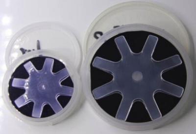
2 type semi isolant gaufrette factice de pouce 50mm N de phosphure d'indium d'INP
Prix: by case
MOQ: 3pcs
Heure de livraison: 3-4weeks
Marque: zmkj
Souligner:gaufrette de phosphure d'indium de 50mm, Gaufrette semi isolante de phosphure d'indium, type gaufrette de n d'INP
gaufrette principale factice de type n de phosphure d'indium d'INP de catégorie de 2inch dia50.8mm
gaufrette semi-isolante d'INP de phosphure d'indium 4inch pour la diode laser de LD, gaufrette de semi-conducteur, gaufrette d'INP 3inch, substrats d'INP du monocristal wafer2inch 3inch 4inch pour l'a... Voir plus
➤ Visiter Site Internet
Haute gaufrette extérieure réfringente de germanium de DSP GE
Prix: by case
MOQ: 3pcs
Heure de livraison: 1-4weeks
Marque: zmkj
Souligner:Gaufrette extérieure de germanium de DSP, haute gaufrette réfringente de germanium, Gaufrette extérieure de GE de DSP
le type type de 2inch 4inch 6inch N de P a enduit des gaufrettes de monocristaux de germanium,
Plats optiques de monocristaux de germanium
Fenêtre de la gaufrette de GE/GE
Le germanium (GE) est le matériel préféré de lentille et de fenêtre pour les systèmes infrarouges de représentation ... Voir plus
➤ Visiter Site Internet
Ge Optical Inp Wafer , Semiconductor Device Indium Phosphide Wafer
Prix: by case
MOQ: 3pcs
Heure de livraison: 1-4weeks
Marque: zmkj
Souligner:Ge Optical inp wafer, Ge Optical Indium Phosphide Wafer, semiconductor device inp wafer
Gaufrettes de monocristaux de germanium, plats optiques de GE
Substrats de germanium
Application : gaufrette de germanium utilisée dans la production du dispositif de semi-conducteur, circuit optique de rayon infrarouge, matériel de descente de pile solaire.
Termes principaux de propriét... Voir plus
➤ Visiter Site Internet
Cube Crystal Mgo Substrates, cristal en croissance de la France d'arc d'oxyde de magnésium
Prix: by case
MOQ: 10pcs
Heure de livraison: 1-4weeks
Marque: zmkj
Souligner:Substrats de MgO de la France d'arc, Cubez les substrats en cristal de MgO, cristal d'oxyde de magnésium de MgO
Substrats de MgO, gaufrette de MgO de 10X10mm, gaufrette de semi-conducteur, substrat en cristal de l'oxyde de magnésium (MgO), GAUFRETTE 5x5mm de MgO de fournisseur de cristauxDescription de produit :L'oxyde de magnésium (MgO) est excellent pour le substrat monocristallin est très utilisé dans la p... Voir plus
➤ Visiter Site Internet

La gaufrette de phosphure d'indium de monocristaux de germanium a adapté la lentille aux besoins du client optique 4/6 pouces de GE
Prix: by case
MOQ: 3pcs
Heure de livraison: 1-4weeks
Marque: zmkj
Souligner:gaufrette d'INP, Gaufrette de Gap
gaufrettes de substrats de GE de monocristaux de germanium de 4inch 6inch, lentille optique adaptée aux besoins du client de GE
Substrats de germanium
Application : gaufrette de germanium utilisée dans la production du dispositif de semi-conducteur, circuit optique de rayon infrarouge, maté... Voir plus
➤ Visiter Site Internet

N / P dactylographient la gaufrette de germanium, le diamètre 0,5 | 150mm de plats d'optique de germanium
Prix: by case
MOQ: 3pcs
Heure de livraison: 1-4weeks
Marque: zmkj
Souligner:gaufrette d'INP, substrat de MgO
le type type de 2inch 4inch 6inch N de P a enduit des gaufrettes de monocristaux de germanium,
Plats optiques de monocristaux de germanium
Fenêtre de la gaufrette de GE/GE
Le germanium (Ge) est le matériel préféré de lentille et de fenêtre pour les systèmes infrarouges de représentati... Voir plus
➤ Visiter Site Internet
Épaisseur primaire/factice 350um de gaufrette de phosphure d'indium de catégorie pour le LD
Prix: by case
MOQ: 3pcs
Heure de livraison: 1-4weeks
Marque: zmkj
Souligner:substrat de MgO, Gaufrette de Gap
2inch gaufrette en cristal factice de type p de type n de substrats d'INP de phosphure d'indium de catégorie de catégorie primaire de l'épaisseur 350um pour le LD
Le matériel de monocristal de phosphure d'indium est un de la plupart de composé important de semi-conducteur, qui est la matière p... Voir plus
➤ Visiter Site Internet

Substrate de germanium GE Fenêtres plates Lentilles optiques Applications d'imagerie thermique et spectroscopie infrarouge Haute dureté
Prix: Negotiable
MOQ: Negotiable
Heure de livraison: 2-4 weeks
Marque: ZMSH
Souligner:Applications d'imagerie thermique Substrate de germanium, Spéctroscopie infrarouge Substrate de germanium, Substrate de germanium à haute dureté
Description du produit
Substrate de germanium GE Fenêtres plates Lentilles optiques Applications d'imagerie thermique et spectroscopie infrarouge Haute dureté
La fenêtre de germanium (Ge) est un matériau chimiquement inerte avec une plage de spectre permise de 2 à 12 μm, qui est un matériau optique... Voir plus
➤ Visiter Site Internet
Dispositif électronique à haute puissance de type épingle à fond plat
Prix: by case
MOQ: Negotiable
Heure de livraison: 2-4weeks
Marque: ZMSH
Souligner:Cu ≥ 99, 9% Substrate de dissipateur de chaleur, Substrate de dissipateur de chaleur à haute puissance
Résumé de cSubstrate de dissipateur de chaleur supérieur
Dispositif électronique à haute puissance de type épingle à fond plat
Le substrat de dissipateur de chaleur en cuivre est un élément dissipateur de chaleur constitué d'un cuivre pur (Cu ≥ 99,9%) ou d'un alliage de cuivre (comme le ... Voir plus
➤ Visiter Site Internet

En tant qu'arsenure d'indium2 pouces 3 pouces 4 pouces Substrate monocristallin N/P Type de semiconducteur Épaisseur de gaufre 300-800um
Prix: Negotiable
MOQ: Negotiable
Heure de livraison: 2-4 weeks
Marque: ZMSH
Souligner:Wafer à l' arsenure d' indium de 4 pouces, Wafer à l' arsenure d' indium de 3 pouces, 2 pouces de gaufre d' arsenure d' indium
Description du produit
En tant qu'arsenure d'indium2 pouces 3 pouces 4 pouces Substrate monocristallin N/P Type de semiconducteur Épaisseur de gaufre 300-800um
L'indium InAs ou indium arsenide monolithique est un semi-conducteur composé d'indium et d'arsenic.L'arsenure d'indium est utilisé pour con... Voir plus
➤ Visiter Site Internet
Substrats de semi-conducteurs à base de plaquettes de gégermanium <111> Concentrer les formes de taille personnalisées du CPV photovoltaïque
Prix: Negotiable
MOQ: Negotiable
Heure de livraison: 2-4 weeks
Marque: ZMSH
Souligner:Wafer de germanium CPV, plaquette de germanium de taille personnalisée, plaquettes de germanium à semi-conducteurs
Description du produit
Substrats de semi-conducteurs à base de plaques de germanium < 111> concentrant des CPV photovoltaïques
Le germanium de haute pureté est dopé avec des éléments trivalents (par exemple, indium, gallium, bore) pour obtenir des semi-conducteurs de germanium de type P,et le... Voir plus
➤ Visiter Site Internet
Oxyde de magnésium Pureté 95% MgO Film Substrate 5x5 10x10 20x20 Épaisseur 0,5 mm 1,0 mm Orientation <001> <110> <111>
Prix: by case
MOQ: 10pcs
Heure de livraison: 1-4weeks
Marque: zmkj
Souligner:5x5 MgO film de substrat, 20 x 20 MgO film de substrat, 10x10 MgO film de substrat
Purification de l'oxyde de magnésium 95% film de substrat 5x5 10x10 20x20 épaisseur 0,5 mm orientation 1,0 mm <001> <110> <111> Description du produit:
L'oxyde de magnésium (MgO) monocristallin de substrat à film mince est un matériau de substrat de haute qualité présentant d'ex... Voir plus
➤ Visiter Site Internet
InAs Wafer Dopé Zn 2 pouces Indium Arsenide Wafer Dia 50mm Épaisseur 500um <100> Personnalisé
Prix: Negotiable
MOQ: Negotiable
Heure de livraison: 2-4 weeks
Marque: ZMSH
Souligner:Wafer à base d'arsenure d'indium personnalisé, 2 pouces de gaufre d' arsenure d' indium, Plaquettes à l'arsenure d'indium de 500um
Wafer épitaxial InAs de 2 pouces pour une diode laser LD, wafer épitaxial semi-conducteur, wafer InAs-Zn de 3 pouces,Plaquettes monocristallines InAs de 2 pouces 3 pouces 4 pouces InAs-Zn sous-strats pour une application LD, plaquette à semi-conducteurs, plaquette épitaxielle au laser à l'arsenure d... Voir plus
➤ Visiter Site Internet
Wafer DFB N-InP substrat épiwafer couche active InGaAlAs/InGaAsP 2 4 6 pouces pour le capteur de gaz
Prix: Negotiable
MOQ: Negotiable
Heure de livraison: 2-4weeks
Marque: ZMSH
Souligner:Epiwafer à substrat InP de 2 pouces, Epiwafer de substrat InP de 4 pouces, Epiwafer à substrat InP de 6 pouces
Wafer DFB N-InP substrat épiwafer couche active InGaAlAs/InGaAsP 2 4 6 pouces pour le capteur de gaz
Rapport de l'épi-plaque de substrat N-InP de la plaque DFB
Une plaque à rétroaction distribuée (DFB) sur un substrat à phosphure d'indium de type n (N-InP) est un matériau critique utilisé dans ... Voir plus
➤ Visiter Site Internet